| Procedure | Item | Capability Indicators | Remarks |
| Panel routing edge width | Three to four layers (bottom copper H or 1OZ) | HOZ ≥ 10 mm /1OZ≥ 12 mm | Edge glue dams are recommended for board perimeter containment |
| Six to eight layers (bottom copper H or 1OZ) | HOZ ≥ 12 mm /1OZ≥ 15 mm | Edge glue dams are recommended for board perimeter containment |
| Ten layers or more (bottom copper H or 1OZ) | ≥ 18 mm | Edge glue dams are recommended for board perimeter containment |
| Four layers (bottom copper ≥ 2OZ) | ≥ 18 mm | Edge glue dams are recommended for board perimeter containment |
| Six to eight layers (bottom copper ≥ 2OZ) | ≥ 18 mm | Edge glue dams are recommended for board perimeter containment |
| Ten layers or more (bottom copper ≥ 2OZ) | ≥ 18 mm | Edge glue dams are recommended for board perimeter containment |
| Lamination | Size(Max) | 840mm*620mm | |
| Number of board layers(Max) | 3—20 layers | |
| Inner core board thickness(㎜) | 0.1mm—3.0mm | 0.1mm does not contain copper, copper thickness ≤ 6OZ |
| Incoming material layer deviation control requirements(mil) | Four layers: 2mil, six layers (inclusive)
and above: 1mil | |
| Item | Ordinary Tg140 | Tg170 | Non-halogen |
| model | 7628 | 7628 | 7628 | 2116 | 2116 | 1080 | 1506 | 3313 | 106 | 7628 | 2116 | 1080 | 2116 | 1080 |
| Content(RC) | 43% | 45% | 48% | 53% | 55% | 65% | 45% | 54% | 72% | 45% | 53% | 65% | 53% | 65% |
| Thickness(um) | 175 | 195 | 215 | 115 | 125 | 75 | 150 | 100 | 50 | 185 | 115 | 75 | 115 | 75 |
| Tolerance(um) | ±15 | ±15 | ±15 | ±15 | ±15 | ±10 | ±10 | ±15 | ±10 | ±15 | ±15 | ±10 | ±15 | ±10 |
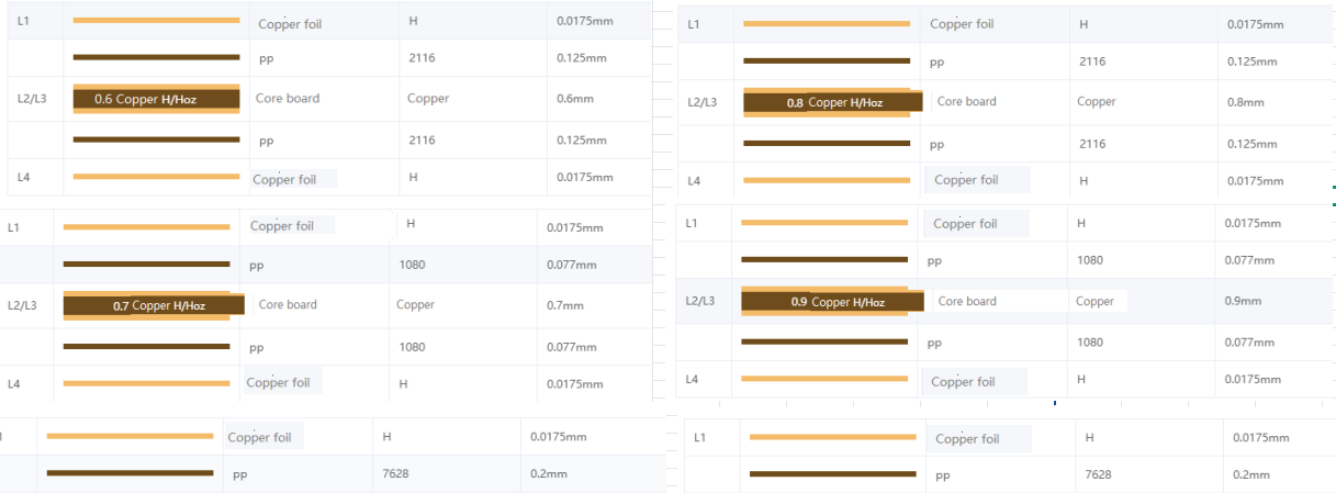
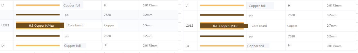
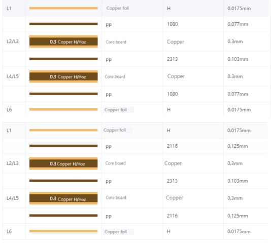
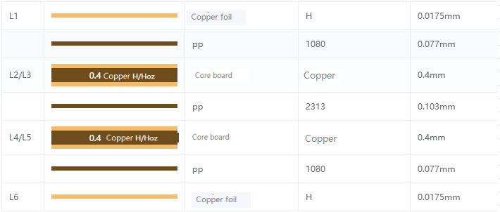
| Laminate thickness(㎜) | 0.30mm — 4.5mm | Additional copper plating on core material must be specified in the MI |
| Laminate tolerance(㎜) | ≤1mm± 0.075㎜ >1mm± 0.10㎜ |
| Hole to line/copper distance | ≥6mil |
| Photoimageable PCB | Dielectric layer | Dielectric layer>0.5㎜ | There is a risk of uneven thickness of multiple PP sheets. It is recommended to add smooth sheets. |
| Riveted PCB | Dielectric layer≥2 times the thickness of the core board | Smooth sheets are needed |
| Basic PP compounding principles | Inner copper
thickness | Number of layers | Outer PP | Middle PP | Amount of PP used | Remarks |
| 1OZ | 4 | 1 | | 2 | 1. When the copper thickness of the inner core board is ≥1OZ, try to use PP with high glue content;
2. When the copper thickness of the inner core board is ≥2OZ, due to the uneven copper plating thickness, there will be a certain difference between the actual configuration of PP and the actual pressing thickness when calculating the thickness;
3. The PP configuration principle in the left figure ensures that the residual copper rate is ≥75% or more; for residual copper rate ≤75%, the PP structure should be reasonably configured after looking at the specific distribution of the physical board graphics;
4. The PP batching principle in the left figure is for reference only. The specific number of outer and interlayer PP is mainly determined by the residual copper rate and copper thickness of the circuits on both sides of the interlayer;
5. When the surface treatment is gold plating and gold immersion process, PP should try to use fine cloth-textured semi-cured sheets. |
| 6 | 1 | 1 | 3 |
| 8 | 1 | 2 | 4 |
| 10 | 1 | 3 | 5 |
| 2OZ | 4 | 2 | | 4 |
| 6 | 2 | 3 | 7 |
| 8 | 2 | 6 | 10 |
| 10 | 2 | 9 | 13 |
| 3OZ | 4 | 3 | | 3 |
| 6 | 3 | 4 | 10 |
| 8 | 3 | 8 | 14 |
| 10 | 3 | 12 | 18 |