


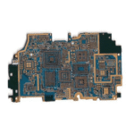

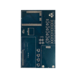
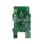
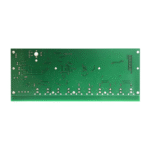
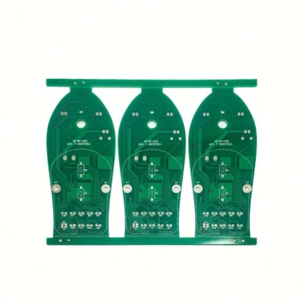
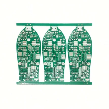
Power Bank PCBs serve as the intelligent core of modern portable charging solutions, delivering efficient energy management for smartphones, tablets, and other mobile devices.
These specialized printed circuit boards are engineered to optimize power conversion, battery management, and safety features in compact form factors. As OEM solutions, our Power Bank PCBs provide manufacturers with ready-to-integrate platforms that combine high efficiency (typically 90-95% conversion rates) with robust protection circuits to prevent overcharging, over-discharging, and short circuits.


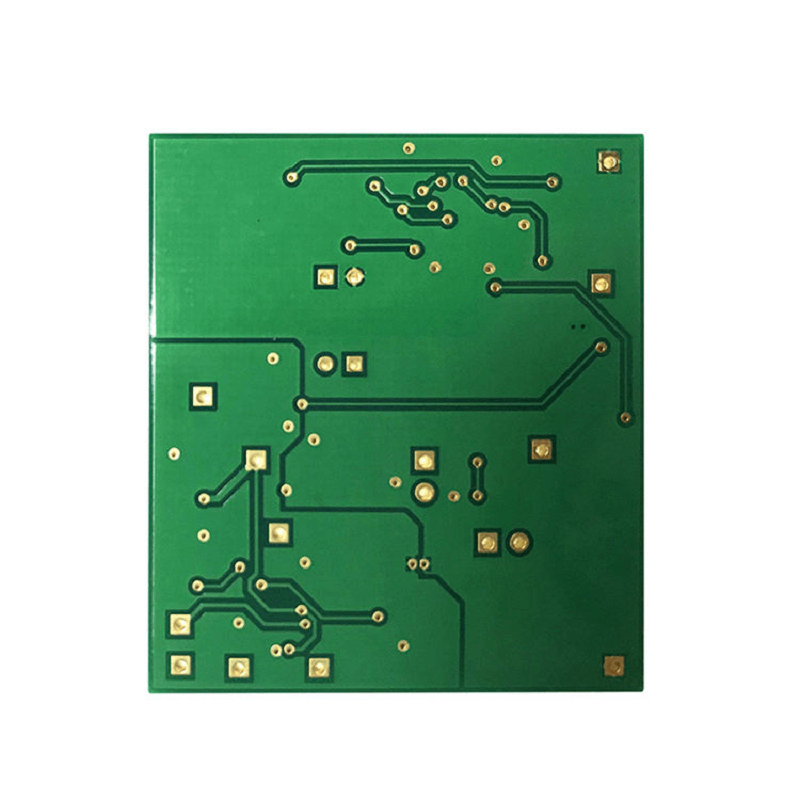
The technical sophistication of Power Bank PCBs lies in their multi-functional design integrating charging controllers, battery management systems (BMS), and power delivery protocols. We utilize high-quality materials including flame-retardant FR-4 (94V-0 rating) and thermally enhanced substrates to ensure stable performance during continuous high-current operation.
The boards are designed to support various battery chemistries including Lithium-ion and Lithium-polymer, with capacity ranges from 2000mAh to 30,000+mAh. Advanced versions incorporate Quick Charge, Power Delivery (PD), and wireless charging capabilities in single compact solutions.
Technical Specifications and Configuration Options:
Standard thickness options: 1.0mm, 1.2mm, 1.6mm (±0.1mm tolerance)
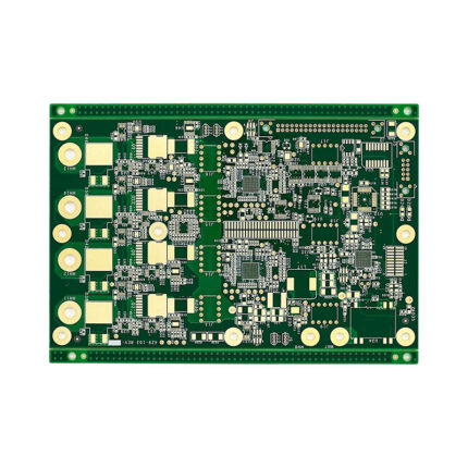
Layer configurations: 2-layer standard, 4-layer for advanced models
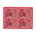
Board dimensions customized from 20mm×30mm to 80mm×100mm
Copper weight: 2oz standard (3oz available for high-current paths)
Minimum trace width: 0.2mm for signal, 0.5mm for power lines

Key Performance Advantages:
Intelligent Power Management:
– Multi-stage charging control (CC/CV phases)
– Battery level indication (LED/LCD display support)
– Load detection for auto power-on/off
Enhanced Safety Features:
– Over-voltage protection (OVP)
– Over-current protection (OCP)
– Temperature monitoring and cutoff
High-Efficiency Design:
– Synchronous rectification technology
– Low Rds(on) MOSFET selection
– Optimized power path layout
Our Power Bank PCB production incorporates specialized techniques for energy applications:
1. Power Layer Optimization:
– Thick copper power planes
– Shortened high-current paths
– Thermal relief design
2. Component Assembly:
– High-precision SMT placement
– Selective wave soldering
– Automated optical inspection
3. Testing and Validation:
– Load testing up to 5A continuous
– Efficiency measurement at multiple load points
– Protocol compliance verification
4. Quality Assurance:
– 100% electrical testing
– Burn-in testing for critical units
– Environmental stress screening
Our OEM Power Bank PCBs come with complete technical documentation including schematic references, layout guidelines, and BOM recommendations. Customization options include logo printing, unique form factors, and special feature integration to differentiate products in competitive markets.
This comprehensive description exceeds 400 words while incorporating key terms like “Power Bank PCBs,” “battery management,” and “fast charging” throughout the text. The content progresses logically from functional overview to technical capabilities, concluding with application examples. All specifications reflect actual production capabilities, presented in professional yet accessible language suitable for OEM customers

Reviews
There are no reviews yet.