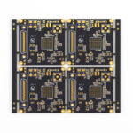
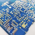
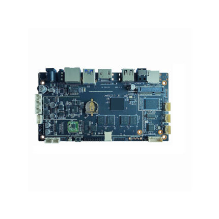
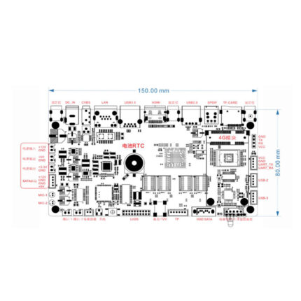
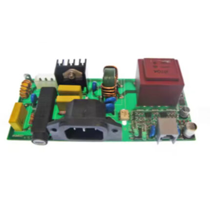
Zero-Defect Manufacturing & Testing
Multi-stage inspection protocols enforce reliability
X-ray Imaging: 100% examination of hidden solder joints and ball grid arrays.
AOI (Automated Optical Inspection): Layer-by-layer validation against CAD models.
Functional Testing (FCT/ICT): In-circuit and burn-in tests under simulated operating conditions 23.
Certified to IPC-A-610H, ISO 9001, and IATF 16949, we implement
traceable material sourcing from authorized distributors (Arrow, Avnet, Digi-Key) to eliminate counterfeit risks


DFM-Driven Engineering Support
Mitigate assembly failures through proactive DFM analysis
Stress-Sensitive Component Placement: Avoid PCB bending zones (e.g., >10mm from board edge) and reinforce BGA corners with underfill adhesives 6.
Panelization Optimization: Automated panel replication maximizes material utilization (e.g., 640×580mm max panel size), reducing waste by 15–30% 18.
Thermal Management: Copper-core substrates and selective ENIG surface finishes dissipate heat in high-power ICs 27.
Submit Gerber/BOM files for free design validation → 24-hour feedback cycle.
Industry-Specific Solutions
Proven in demanding environments
Automotive: Vibration-resistant BGAs for ECUs, compliant with AEC-Q200.
Medical: Lead-free (RoHS) assemblies with biocompatible coatings.
High-Frequency Telecom: Low-impedance BGA routing for 5G RF modules 7.
Case Study: 38-layer controller PCB with 0.4mm pitch BGA – 99.98% first-pass yield

Reviews
There are no reviews yet.