


From Prototype to Production: Multilayer PCBs That Deliver Performance and Reliability
With continuous advancements in materials and processing technologies, our multilayer PCBs deliver increasingly sophisticated solutions for electronic packaging challenges. The combination of precision layer stacking, advanced via structures, and optimized signal paths enables designers to push the boundaries of performance while maintaining reliability. From prototype development to volume production, our multilayer PCB solutions provide the interconnect foundation for tomorrow’s electronic innovations.
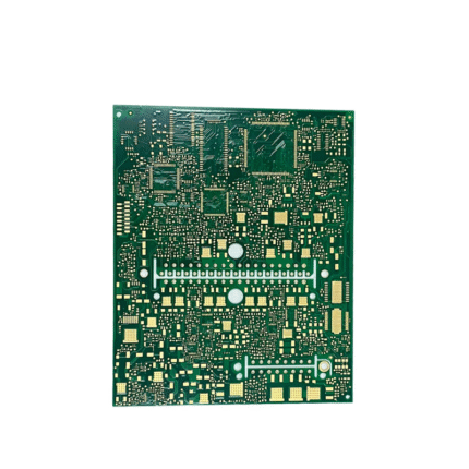
Optimized Signal Integrity and Space with Multilayer PCBs
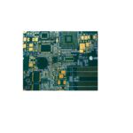
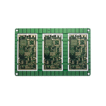
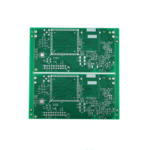
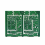
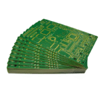
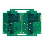
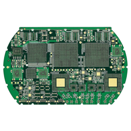
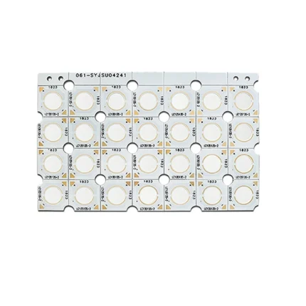
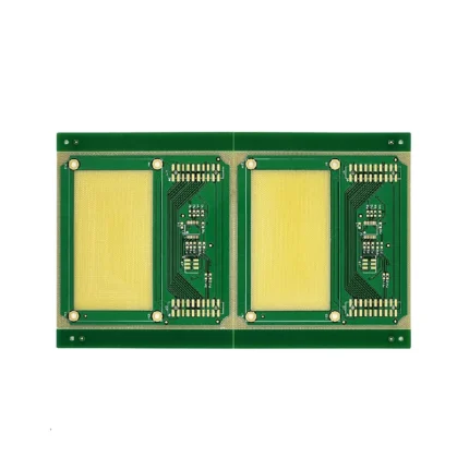
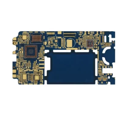
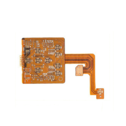
Multilayer PCBs represent the cornerstone of modern electronics, enabling sophisticated circuit designs that power today’s most advanced technologies. These complex printed circuit boards integrate multiple conductive layers (typically 4 to 50 layers) separated by dielectric materials, providing the necessary interconnect density for high-performance computing, telecommunications infrastructure, medical equipment, and aerospace systems.
Unlike simple single or double-sided boards, multilayer PCBs offer superior signal integrity, reduced electromagnetic interference (EMI), and optimized space utilization – critical features for compact, high-speed electronic devices.


Engineered Precision: Materials and Methods Behind Multilayer PCBs
The multilayer PCB manufacturing process requires precision engineering to ensure reliable layer-to-layer connections and consistent electrical performance. Our multilayer boards utilize high-quality materials including FR-4, high-speed laminates (such as Megtron 6 or Isola FR408HR), and specialized substrates for RF applications. These materials are carefully selected based on dielectric constant (Dk 3.5-4.8), dissipation factor (Df 0.001-0.02), and thermal properties (Tg 140-220°C) to meet specific design requirements.
Comprehensive Quality Assurance for Every PCB We Build
Electrical Testing:
– 100% netlist verification
– Hi-Pot testing (up to 1000V DC)
Impedance Control:
– TDR (Time Domain Reflectometry) testing
– Coupon-based verification
Microsection Analysis:
– Plating thickness measurement
– Interconnect integrity inspection
Thermal Stress Testing:
– 6× thermal cycles (-55°C to +125°C)
– Solder float testing (288°C, 10 sec)

Reviews
There are no reviews yet.