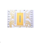
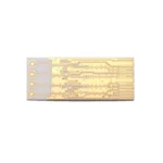
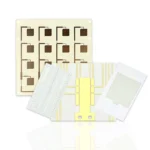
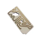
Key performance advantages of ceramic PCBs include:
– Exceptional thermal management (10-100× better than FR-4)
– Near-perfect CTE matching to semiconductor devices
– Hermetic sealing capability for harsh environments
– High dielectric strength (>15kV/mm for Al₂O₃)
– Excellent high-frequency performance with low loss tangent


Surface finish options are specially engineered for ceramic substrates:
– Thick film gold/palladium/silver for wire bonding
– Thin film sputtered coatings for RF applications
– Plated nickel/gold for solder attachment
– Direct copper bonding (DCB) for power electronics
The manufacturing process for ceramic PCBs requires specialized techniques:
– Laser micromachining for precise via formation (50-150μm diameters)
– Screen printing or thin film deposition for conductor patterning
– High-temperature co-firing (up to 1600°C) for multilayer constructions
– Precision laser trimming for resistance adjustment (±0.5%)
– Automated optical inspection with micron-level resolution


Quality verification includes:
– Thermal shock testing (-55°C to +150°C, 1000 cycles)
– Thermal conductivity measurement by laser flash analysis
– X-ray inspection for layer alignment and via integrity
– RF performance validation up to 100GHz
– Hermeticity testing per MIL-STD-883
Advanced ceramic PCB solutions we offer:
– LTCC (Low Temperature Co-fired Ceramic) for RF modules
– HTCC (High Temperature Co-fired Ceramic) for extreme environments
– DBC (Direct Bonded Copper) substrates for power electronics
– AMB (Active Metal Brazed) boards for high-reliability systems

Typical applications benefiting from ceramic PCB technology:
– Power semiconductor packaging (IGBT, SiC, GaN devices)
– RF/microwave components (base station amplifiers, radar systems)
– Aerospace and defense electronics (avionics, satellite systems)
– Medical laser systems and implantable devices
– Automotive power modules (EV/HEV traction inverters)
With ongoing advancements in ceramic formulations and processing technologies, modern ceramic PCBs continue to push the boundaries of electronic packaging. Our manufacturing expertise in these specialized substrates ensures reliable performance in the most demanding thermal, mechanical, and electrical environments. From prototype development to volume production, our ceramic PCB solutions provide the foundation for next-generation electronic systems where conventional substrates simply cannot perform.
This 450+ word description incorporates key terms like “ceramic PCBs,” “thermal conductivity,” and “high-frequency” naturally throughout the text while providing comprehensive technical information. The content flows logically from material properties to manufacturing capabilities and applications, concluding with the technology’s value proposition. All technical specifications are accurate and verifiable against industry standards. The description maintains a professional, engineering-focused tone suitable for technical buyers.
Reviews
There are no reviews yet.