


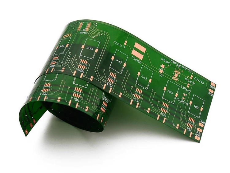
Wearable devices continue to become smaller, lighter, and more functional. Smartwatches, fitness trackers, medical monitoring devices, and wireless accessories must accommodate sensors, batteries, processors, and communication modules within limited internal space. Traditional rigid circuit boards can restrict component placement and increase the difficulty of designing compact enclosures. A polyimide flexible PCB circuit board provides an alternative by allowing electronic connections to follow curved surfaces and fit into narrow spaces.
Polyimide is widely used in flexible electronics because of its thermal resistance, mechanical flexibility, and dimensional stability. Unlike conventional rigid substrates, flexible materials can bend to match the internal geometry of a device. Consequently, engineers can reduce unnecessary board space and improve the use of available enclosure volume. This flexibility also creates more opportunities for lightweight product designs.
How Polyimide Materials Improve Space Utilization
The main advantage of polyimide is its ability to support thin and flexible circuit structures. For wearable products, every millimeter of internal space can influence battery capacity, component placement, and overall product dimensions. Flexible circuits can connect components positioned on different surfaces without requiring several separate rigid boards. As a result, designers can simplify internal layouts and reduce the space occupied by interconnections.
Polyimide also provides useful thermal and mechanical properties for compact electronics. Wearable devices may experience repeated movement, temperature changes, and continuous daily use. Therefore, the substrate must maintain reliable electrical connections under the intended operating conditions. With suitable material selection and circuit construction, flexible boards can support compact designs without sacrificing essential functionality.
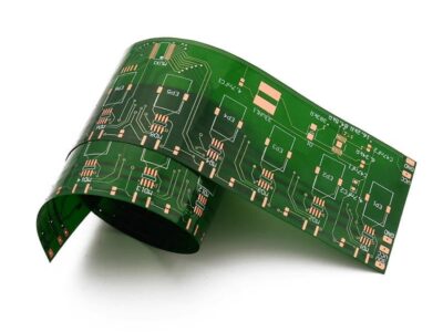
Key Design Factors for Flexible PCB Space Savings
Effective space optimization requires more than choosing a flexible substrate. Engineers must consider layer count, copper thickness, trace spacing, bend radius, and component placement together. A polyimide flexible PCB circuit board can support different layouts depending on the mechanical structure and electrical requirements of the final product. However, the design must also protect conductive traces from excessive bending stress.
Several design considerations can help improve wearable device layouts:
- Optimize circuit routing: Arrange traces to follow the available internal space and avoid unnecessary routing paths.
- Select suitable layer counts: Use multilayer structures when additional routing density is necessary, while balancing thickness and manufacturing complexity.
- Control bend radius: Maintain an appropriate bending radius to reduce stress on copper traces and the substrate.
- Minimize unnecessary connectors: Use flexible interconnections where practical to reduce additional components and assembly space.
- Consider component placement: Position components strategically to avoid mechanical interference during device assembly.
These design decisions should be evaluated together rather than independently. Furthermore, early collaboration between mechanical and electrical engineers can prevent enclosure conflicts and improve assembly efficiency.
Flexible PCB Manufacturing Specifications and Capabilities
Different wearable products require different circuit dimensions and electrical configurations. FPC flexible PCBs can support compact layouts, while double-sided and multilayer designs provide additional routing options. The following specifications illustrate the available manufacturing capabilities for flexible circuit projects.
| Parameter | Available Specification | Design Benefit |
|---|---|---|
| Base materials | Polyimide; LCP for high-frequency applications | Supports different electrical and mechanical requirements |
| Thickness | 0.05–0.3 mm | Enables thin and lightweight circuit structures |
| Layer count | 1–8 layers | Accommodates different routing densities |
| Copper weight | 0.5–2 oz; 1 oz standard | Supports different current and circuit requirements |
| Minimum trace/space | 2/2 mil (50 μm/50 μm) | Supports fine-pitch circuit layouts |
| Bend radius | At least 3× material thickness for static applications | Helps guide mechanical design |
These specifications provide flexibility for different product architectures. For example, thin single-layer circuits may suit simple wearable connections, while double-sided flexible PCBs can provide more routing space within a compact structure. In addition, LCP materials may be considered for applications requiring specialized high-frequency electrical performance.
Single-Sided, Double-Sided, and Multilayer Flexible PCB Designs
Single-sided flexible circuits are suitable for relatively simple electronic connections. They can offer a lightweight structure with fewer manufacturing steps, making them useful for cost-sensitive wearable products. However, more complex devices may require additional routing capacity to connect multiple sensors, displays, and control components.
Double-sided flexible PCBs provide conductive patterns on both sides of the substrate. This arrangement increases routing options without requiring multiple separate circuit boards. Meanwhile, multilayer flexible structures can accommodate denser interconnections for advanced wearable electronics. Nevertheless, designers should balance layer count against thickness, flexibility, thermal performance, and fabrication cost.
How Rigid-Flex Integration Supports Advanced Wearable Designs
Some wearable products combine flexible connections with rigid areas for mounting processors, sensors, or other electronic components. Rigid-flex structures bring these functions together within one integrated circuit assembly. This approach can reduce the need for separate connectors and improve packaging efficiency. It is particularly useful when the product contains both fixed components and sections that must bend around the enclosure.
However, rigid-flex board PCBA processing requires careful coordination between PCB fabrication and assembly. Component placement, soldering conditions, mechanical support, and flexible section protection all influence final reliability. Therefore, engineers should define rigid and flexible areas clearly during the design stage. This helps reduce assembly complications and supports more consistent product performance.
Manufacturing Considerations for Reliable Flexible PCB Design
A successful flexible circuit depends on both electrical layout and mechanical construction. A polyimide flexible PCB circuit board should be designed according to its expected bending conditions, installation method, and operating environment. Static bending applications generally require different design considerations from products that experience repeated dynamic movement. In addition, copper thickness and trace geometry can influence the circuit’s ability to withstand mechanical stress.
For reliable flexible PCB design, manufacturers and engineers should evaluate several important factors:
- Material compatibility: Match polyimide or LCP materials with the product’s thermal and electrical requirements.
- Trace geometry: Avoid sharp corners and unnecessary stress concentration in bending areas.
- Thickness control: Select a suitable total thickness for the enclosure and mechanical design.
- Electrical verification: Check continuity and insulation performance before assembly.
- Mechanical testing: Evaluate bending performance under conditions representative of actual use.
These practices help reduce potential failures during product assembly and daily operation. Moreover, design reviews before mass production can identify routing or mechanical problems at an earlier stage.
Choosing a Flexible PCB Manufacturing Partner
Selecting a flexible PCB manufacturing partner requires evaluating material experience, fine-line fabrication capabilities, layer structures, and quality control procedures. Wearable device projects may involve strict space constraints and specialized mechanical requirements. Therefore, manufacturers should be able to support customized thicknesses, circuit dimensions, and flexible or rigid-flex configurations.
Baiyoudi provides flexible PCB manufacturing options using polyimide and LCP materials, with thicknesses from 0.05 mm to 0.3 mm and configurations of up to eight layers. Its fine-line manufacturing capability supports trace and space dimensions down to 2/2 mil. By combining material expertise with customized fabrication, Baiyoudi helps customers develop flexible circuit solutions for compact wearable electronics.
Ultimately, flexible PCB technology allows designers to make better use of limited internal space while supporting lightweight product construction. With appropriate material selection, careful routing, and controlled manufacturing, wearable devices can achieve more compact layouts and reliable electronic connections.